

After getting re-acquainted with the Psion MC400 (and making the machine a little more usable in 2021) I came across some online posts discussing the plausibility of creating an “MC400 Emulator” and this got me thinking… The early iteration of the EPOC16/SIBO OS in this machines is truly a marvel of engineering – squeezing a full multi-tasking GUI into 256k of ROM running on a 7.68MHz 80C86 with 256k of RAM is no mean feat. Just let that sink in for a little while… 256k of RAM – k as in kilobytes, as in 1/4 of a megabyte, as in 1/4000th of a gigabyte… a modern laptop in 2021 might have 16GB of RAM – 256k is 1/65536th of the memory! Copious use of assembler, object-oriented design and code-sharing libraries give the MC400 a solid and polished feel despite its age and limited resources. The (monochrome) GUI is simple and pleasing to work with albeit a little slow by today’s standards.
Almost all of the other Psion SIBO machines already have officially-released “emulators” (S3emul.exe, S3aEMUL.EXE etc.) that run under DOS (or dosbox 😉 ).

In much the same way as Ash Wolf’s excellent work WindEmu (that even lets you run “Series 5 in your browser” 😉 ) the first place to start when looking at emulation is often the ROM…
(Note: Thanks to the work that went into creating the Psion Series 5mx emulator above it was apparently only a small-ish (!) step to getting it running under MAME too. And of course although not actual emulation per se the WINS version of EPOC32 will run on Windows and under Wine).


Meanwhile, back on the MC400 some simple OPL code (or even using Psion’s own “PANSHLL” shell) can list & copy the MC400’s ROM disk contents, so getting the actual files is fairly trivial.

The PANSHLL listing above lists only 170,096 bytes in the ROM files, where’s the other ~86k of space gone…? Obviously the ROM disk is just that – a static image of a disk/file structure, the other space is the bootstrap kernel-like code part of the OS that actually configures base hardware then loads and runs the higher layers (you’ll notice some processes that are displayed as running but their .IMG files are not present in the ROM file list, like SYS$NULL & SYS$MANG for example). To find out exactly we’ll have to look at the binary contents of the ROM chip(s) themselves. Emulators usually require a binary image of the chip contents as they usually contain machine-code instructions that bootstrap the machine before loading any filesystem images where executable programs etc. might be. So the MC400 ROM probably contains some boot code, maybe some low-level drivers (possible decryption or de-obfuscation of the binary contents?) and a separate (maybe DOS/FAT compatible) ~170k disk image of the ROM files listed above.

I have a “spare” MC400: the first one I bought most recently. It’s had a tough life though – the previous owner had left it in storage (in a shed) with a NiCad battery pack in place which has leaked and corroded some of the machine’s internals. I bought another MC400 some months later but kept the 1st one in case I ever needed any spares. I decided to tear down the “spare” and check out the ROM chips.

The MC400 ROM is realised in 2 x Intel 28F010 128k flash chips – not really surprising as these are the same chips used in the early Psion Flash SSDs. I do have the kit to read them but it means de-soldering them and I’m not sure I’m prepared to go there just yet… Matt Gumbley’s EDisAsm tool would be a much more elegant and simple way of dumping a ROM image, but the setup/config of the Topspeed compiler environment and modification of the source to run on the MC is a step too far in terms of the effort & time required. Yay for brute force – de-soldering the chips!

UPDATE: Jan 2023 – finally, code based on Matt Gumbley’s EDisAsm is pressed into service as a ROM dumper 🙂
Reading the EPOC16 (SIBO) SDK & HDK gives some clues to the partitioning of memory/address space and 80C86 register use: “ASIC2 is always used in 16 bit mode” – the 2 flash chips share the address bus and provide 2 x 8bits (High & Low) of data. The ROM image should contain the classic x86 bootstrap instructions in the top 16 bytes of the ROM address space.

The 8×12 keyboard matrix is split between the 61-key Cherry main keyboard and the 8 case-mounted supplementary buttons (Task/Del/Home/End/PgUp/PgDn/LCD/Rec).
Keyboard matrix decoded here during USB-ing the old Cherry keyboard 🙂
Using the “PANSHLL” shell as an investigative tool on the MC400 lists running processes, segments and devices:
ž Psion PLC 1991
Epoc/Os V2.36F Rom V2.60F
Shell V2.07F
Mon/20/Sep/2021 14:18:52
Display is 640 by 400
Old psu. Bat NiCd 600
RAM  SIZE: 256 Kbytes
FREE SIZE: 76 kbytes
$ lproc
List of processes:*
-----------------
SYS$NULL.$01 0200 READY
SYS$MANG.$02 0CA0 SEM
SYS$FSRV.$03 2780 SEM
SYS$WSRV.$04 77D0 SEM
SYS$WSRV.@05 77D0 SEM
SYS$SHLL.$06 2A00 SEM
SYS$NTFY.$07 0E10 SEM
TERM.$08     3140 SEM
LINK.$09     22F0 SEM
SYS$NCP.$10  0EE0 SEM
SYS$RFSV.$11 0A10 SEM
FLMAN.$12    3590 SEM
PANSHLL.$13  3D20 CURRENT
SYS$CON.$14  1A50 SEM
TP.$15       2980 SEM
$ lseg
List of segments:*
----------------
SYS$NULL.$01 0228 0020 01
SYS$MANG.$02 0248 00CA 01
SYS$FSRV.$03 0312 0278 01
SYS$WSRV.$04 058A 077D 01
SYS$SHLL.$06 0D07 02A0 01
SYS$NTFY.$07 0FA7 00E1 01
TERM.$SC     1088 0255 01
TERM.$08     12DD 0314 01
LINK.$SC     15F1 0111 01
LINK.$09     1702 022F 01
SYS$NCP.$SC  1931 0222 01
SYS$NCP.$10  1B53 00EE 01
SYS$RFSV.$11 1C41 00A1 01
FLMAN.$SC    1CE2 022A 01
FLMAN.$12    1F0C 0359 01
PANSHLL.$13  2265 03D2 01
SYS$CON.$14  2637 01A5 01
TP.$SC       27DC 0553 01
TP.$15       2D2F 0298 01
PANSHLL.$SC  2FC7 02C1 01
Total free segments = 100F
$ ldev
List of devices:*
---------------
LDD - ALM (units=-1)
LDD - PRN (units=-1)
LDD - PRD (units=-1)
LDD - LAY (units=-1)
LDD - DBG (units=1)
LDD - CON (units=-1)
LDD - NCP (units=-1)
LDD - HMD (units=-1)
LDD - XMD (units=-1)
LDD - LLC (units=-1)
LDD - MAS (units=-1)
LDD - MCR (units=2)
LDD - PAR (units=2)
LDD - TTY (units=2)
LDD - SND (units=1)
LDD - TIM (units=-1)
LDD - TXT (units=-1)
LDD - FIL (units=-1)
PDD - FSY.REM
PDD - FSY.LOC
PDD - FSY.ROM
PDD - LOC.TYM
PDD - LOC.TY2
PDD - LOC.TY1
PDD - LOC.TY0
PDD - TTY.HSS
PDD - TTY.UAR
$
Interesting points:
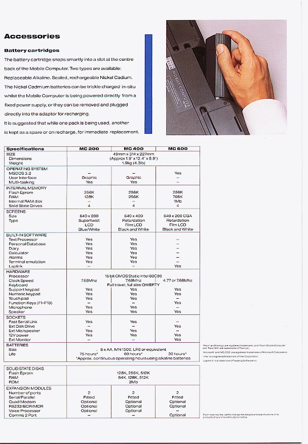
Note the VAX/VMS influence in the “SYS$...” process naming (and hiding from ordinary users) of system processes.TTY.HSS – is the “High Speed Serial” port – not sure if any HSS peripherals were ever released that would be supported by the MC400, the MC range brochure shows an external 3.5″ 1.44M floppy drive that looks like it might be plugged into this interface on the MC600 (DOS-version) although the MC600 is different hardware (no touchpad, extra row of Fn keys):

Nope – looks like the MC600 doesn’t have the HSS after all:
Next steps: poking around via _x86 machine code in the MC400’s internals, and/or picking up some of the SIBO-Linux project’s work/tools from Matt Gumbley’s page…


Nice work! Is there any way to upgrade the RAM on the MC400 ? (desolder existing and modify the board?)
Good question – I’m sure it might be possible to physically replace the chips with versions with more storage but if the architecture is limited to an 18 bit bus for the RAM or the OS assumes a fixed 256k then it might be a waste of time & effort. Some of the block diagrams for the SIBO system seems to imply that the “16 bit memory” block has a 20 bit wide address bus giving a theoretical max memory of 1M, but this would include both RAM & ROM.
I know that the later 16-bit Psion machines (Series 3a/c/mx & Workabout) use bank-switching techniques to address RAM sizes up to 2M, but the MC pre-dated those machines by many years.